A recognized expert in electrical power and advanced materials, Mersen enables the performance and reliability of industrial systems and essential infrastructure across a range of areas, from power management and electric vehicles to renewable energies and storage, aerospace and rail.
As a major player at the heart of technology, Mersen is a committed partner to the companies that drive the industry forward and shape a more sustainable society.
Joining Mersen means joining an international industrial company firmly anchored in today’s real world but with its sights set firmly on the future. It means joining a world of diversity, in terms of professions, technologies, projects and cultures, and a working community with real expertise to help forge tomorrow’s world.
Mersen: high purity graphite for semiconductor and PV industry controlled with the ETV ICP OES method
Mersen: high purity graphite for semiconductor and PV industry controlled with the ETV ICP OES method
Documentation
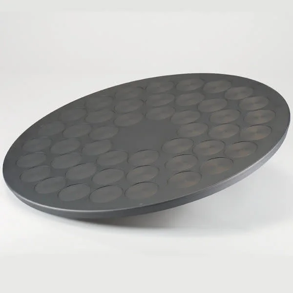
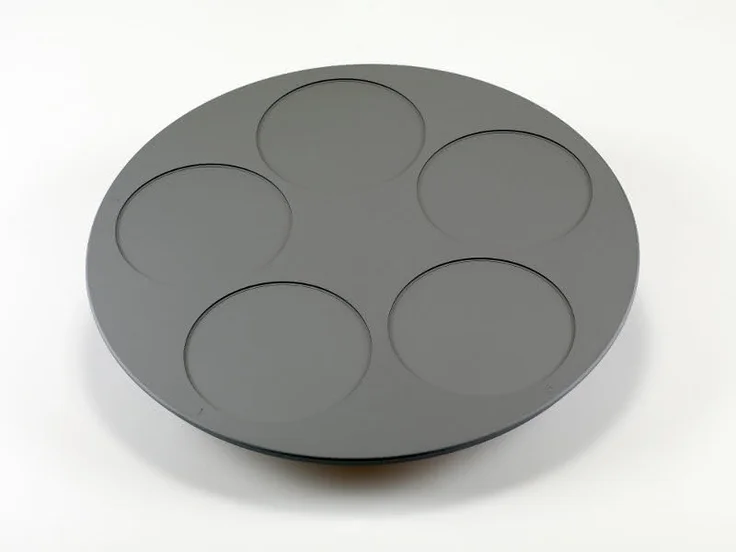
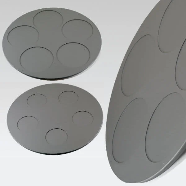
High purity graphite
Mersen has developed processes designed to significantly improve the physicochemical properties of materials, particularly when required for high-tech applications subjected to high stresses.
Mersen offers the ETV-ICP (Electro Thermal Vaporization & Inductively Coupled Plasma) analytical method to measure the graphite purity.
High-tech constraints of semiconductor and PV industries
Purity constraints:
Our purity processes allow us to achieve extremely low impurity levels, to below 5 ppm.
The ETV-ICP method is used to detect and monitor impurities to levels below 5 ppb.
Cleanliness constraints:
Vitreous Carbon Impregnation (VCI) was developed to reduce particle emissions and the vacuum outgassing of materials, particularly for semi-conductor applications.
Resistance to reagents used in plasma processes:
Mersen products can be coated with a thin layer of pyrolitic carbon thereby reducing the material's permeability to reactive products to a minimum, particularly for semi-conductor applications.
In order to further enhance the resistance to process reagents, Mersen proposes core impregnation with resin to reduce porosities.
Resistance to hydrogen above 900 °C, MOCVD reagents, and strong acids (HCL, HF)
Mersen has mastered the deposition of silicon carbide thin films which provides unequalled protection of graphite equipment in particularly harsh environments.