
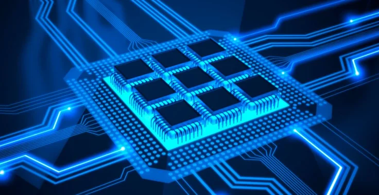
Mersen: leading the way in cutting-edge semiconductors
At the heart of the rapidly evolving semiconductor market, Mersen stands as a beacon of innovation and reliability.
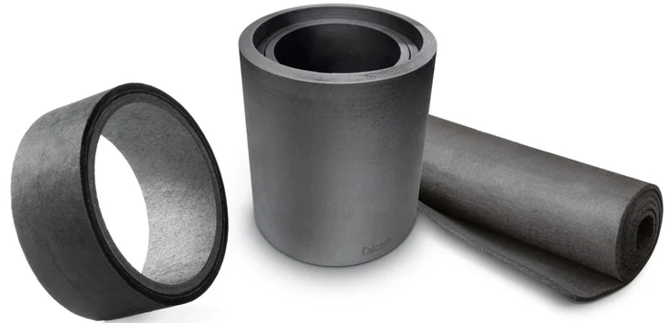
With our expertise in graphite and insulation felts for semiconductors manufacturing process, we are uniquely positioned to meet the industry's growing demands for efficiency and performance.
Our advanced materials and technologies are shaping the future of semiconductors, driving progress in an ever-advancing digital world.
-
Key facts
Mersen for confidence, reliability and performance
We understand the importance of material reliability and durability in semiconductors. That's why Mersen is a true partner for semiconductors manufacturing.-
15.00 %
of energy savings with graphite CALCARB EDGE solutions
-
24.00
R&D centers around the world
-
-
Focus on
Epitaxy in semiconductors manufacturing
Epitaxy is a sophisticated manufacturing process that involves the precise deposition of crystalline layers onto a substrate to form semiconductor devices. This method is crucial for creating a layered structure where each layer's atomic arrangement mirrors that of the substrate beneath it. Two key aspects of this process are the precise control of temperature and the use of specific silicon-based compounds.
Precise temperature control
Epitaxy is a high-temperature process, and maintaining exact temperature control within the epitaxy reactors is crucial. The quality of the crystalline layers and, consequently, the performance of the semiconductor devices depend significantly on this precise temperature management. Mersen's advanced graphite solutions play a vital role here, offering exceptional thermal stability that helps maintain consistent temperatures throughout the process.
Use of silicon-based compounds
The epitaxial growth process typically involves silicon-based compounds such as silicon (Si), silicon-germanium (SiGe), and silicon phosphorus (SiP). These materials are selected based on their ability to tailor the electronic characteristics of each layer, which is essential for the functionality of devices like integrated circuits. The choice of materials directly influences the electrical and physical properties of the semiconductor devices, making the selection process integral to semiconductor manufacturing.
-
Exceeding performance expectations and driving innovation
Amelia Johnson
Senior Process Engineer
I've seen firsthand how Mersen' solutions have transformed our semiconductor production. Their materials consistently exceed our performance expectations, driving innovation in our high-power applications. -
Mersen Inside
SiC power semiconductor manufacturing process
Transcription
Mersen is not visible in the final product, yet it plays a crucial role in the SiC power semiconductor manufacturing process.
In today's world, and even more so in tomorrow's, SiC power semiconductors are at the heart of number of equipment: in renewable energies, electric vehicles, industrial drive and motors... Without these hundreds of tiny components, designed to switch electric currents at a very high level, nothing would work.
Now, the SiC semiconductor manufacturing is terribly complex, tough and meticulous: from SiC sublimation growth to cutting of wafers into chips, via epitaxy and ion implantation, each stage is subject to performance and cost challenges.
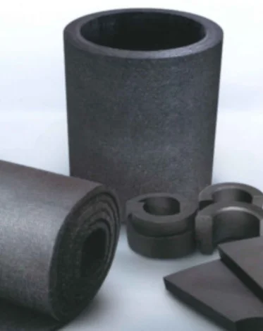
Within this manufacturing process, the quality of the material is key. A leading expert in advanced materials, Mersen supplies fine grade graphite and thermal insulation for furnace linings, wafer carriers in graphite for epitaxy and electrodes in graphite for ion implantation.
Our strengths: our ULTRA-HIGHLY PURIFIED GRAPHITE and high-performance insulation with exceptional qualities:
- Thermal resistance at SiC melting point (Resistance to High temperature up to 2400°C)
- Ability to prevent contamination (High corrosion and chemical resistance)
- Resistance against aggressive media (Outstanding durability)
- Ability to machine intricate and precise design (Fine grain & high machining precision)
- Customization at every stage (grades, machining, purification, coatings)
Thanks to this “magical materials”, that improves efficiency and ensures top-quality SiC substrate, Mersen is a key partner for SiC wafer manufacturers. -
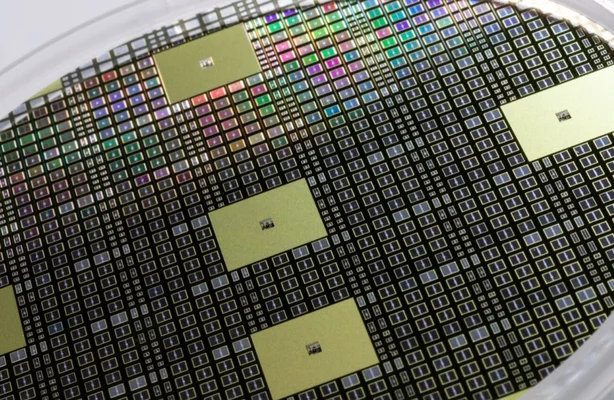
1- Polysilicon manufacturing
The journey begins with polysilicon manufacturing, a critical component in silicon wafer manufacturing. Two primary methods are employed: the Siemens process and the Fluidized Bed Reactor (FBR). In the Siemens process, ultra-pure graphite electrodes from Mersen are used in a reactor chamber where silicon rods are heated and exposed to gaseous trichlorosilane (TCS), resulting in the deposition of pure silicon. The FBR method, on the other hand, involves silicon micro-grains reacting with silane in a heated reactor, producing pure silicon in bead form.
2- Silicon crystal growth
The next stage is silicon crystal growth, a process pivotal in epitaxy and silicon wafer manufacturing. This stage involves methods like Czochralski (CZ) where Mersen's solutions, including isostatic graphite crucibles and graphite felt insulation, play a vital role. These materials ensure the controlled environment necessary for perfect crystal growth, a cornerstone in semiconductor fabrication.
3- Deposition or epitaxy on wafer
Deposition or epitaxy on the wafer is where layers of silicon are precisely deposited to form the semiconductor's base. This stage requires high purity and precision, areas where Mersen's expertise in materials like CVD Silicon Carbide and silicon carbide becomes indispensable.
4- Photolithography: patterning the silicon wafer
Photolithography is a critical process in semiconductor manufacturing that involves transferring intricate circuit patterns onto a silicon wafer. It starts with applying a light-sensitive chemical layer called photoresist to the wafer's surface. Then, the wafer is exposed to ultraviolet light through a photomask, which holds the desired circuit pattern. Based on the type of photoresist used (positive or negative), the light causes a chemical change in the exposed areas. For positive photoresist, these areas become soluble, while for negative photoresist, they harden. Next, the wafer undergoes a development process that removes either the exposed or unexposed regions of the photoresist, depending on the type used. This step effectively transfers the circuit pattern from the photomask to the wafer.
5- Precision etching for circuit definition
Precision etching is then used to define the circuit on the silicon wafer. This process involves removing excess material, a step where the durability and resistance of materials to high temperatures and corrosive environments are crucial.
6- Ion implantation for local modification
During this stage, ions of specific elements are accelerated under an electric field and directed into the silicon substrate. This process allows for precise control over the depth and concentration of the implanted ions. The primary purpose of ion implantation is to introduce dopants into the silicon wafer, which alters its electrical conductivity.
7- Activating elements with annealing techniques
Annealing is a subsequent process that follows ion implantation in semiconductor manufacturing. This technique involves heating the silicon wafer to a high temperature and then slowly cooling it down. The primary purpose of annealing is to activate the dopants that were introduced during ion implantation. By heating the wafer, the dopant atoms are enabled to move into substitutional positions within the silicon lattice, thereby becoming electrically active. Annealing also helps repair the damage to the silicon crystal structure caused by the ion implantation process.
8- Wafer dicing and packaging
The wafer is diced into individual chips and packaged. This final stage marks the culmination of the semiconductor manufacturing process, where each of Mersen's contributions in materials and technology come together to produce the final high-quality semiconductor product.
-
Semiconductors
Need to get information on semiconductors manufacturing solutions?
-
How to enhance semiconductors and silicon wafer manufacturing?
Enhancing silicon wafer manufacturing is key to meeting the growing demands of the industry. With advancements in technology, there are several ways to improve the quality, efficiency, and performance of semiconductor wafers.
Improving quality and efficiency in silicon wafer manufacturing
Improving the quality and efficiency in silicon wafer manufacturing involves optimizing various processes, from the purity of materials to the precision of manufacturing techniques. Utilizing high-purity materials is crucial, as impurities can significantly impact the performance of the semiconductor. Additionally, refining manufacturing processes to increase yield and reduce defects is essential. This includes controlling environmental factors such as temperature and contamination, and employing advanced techniques for silicon crystal growth and wafer slicing.
High temp purification of graphite
The purification of graphite involves heating graphite to very high temperatures to remove impurities and enhance its properties. Purified graphite is essential in various stages of semiconductor manufacturing, such as in crucibles for silicon crystal growth and as components in high-temperature furnaces. The purity of graphite directly affects the quality of the semiconductor wafers produced.
Protecting graphite with SiC coating and TaC coating
Protecting graphite components in semiconductor manufacturing is essential due to graphite's susceptibility to oxidation at high temperatures. Applying Silicon Carbide (SiC) and Tantalum Carbide (TaC) coatings to graphite parts enhances their durability and resistance to harsh environments. TaC and SiC coatings protect the graphite from erosion and contamination, thereby extending its lifespan and maintaining the purity required for semiconductor manufacturing processes.
Elevating silicon crystal properties through epitaxy
Epitaxy is a process used to grow crystalline layers on a substrate wafer, and it plays a crucial role in defining the properties of silicon crystals. Elevating silicon crystal properties through epitaxy involves precise control over the deposition of these layers. This control is essential for tailoring the electrical properties of the semiconductor, such as doping concentration and layer thickness. Advanced epitaxy techniques enable the production of semiconductor wafers with superior electronic properties.
Enhancing ALD processes with graphite susceptor
Atomic Layer Deposition (ALD) is a technique used to deposit thin films on wafers with extreme precision. Enhancing ALD processes can be achieved by using graphite susceptors. These susceptors, made of high-purity graphite, provide uniform heating and excellent thermal stability, which are crucial for the ALD process. The use of graphite susceptors ensures consistent film quality and thickness.
Advancing SiC epitaxial layering for enhanced performance
Silicon carbide (SiC) epitaxial layering is a process that significantly enhances the performance of semiconductor devices. SiC offers superior electrical properties, such as higher breakdown electric field strength and thermal conductivity, compared to traditional silicon. Advancing SiC epitaxial layering involves perfecting the deposition of thin SiC layers on substrate wafers, ensuring uniformity and minimizing defects. This advancement is crucial for high-power and high-frequency semiconductor applications.
-
Semiconductors
Silicon carbide (SiC) - the future of semiconductors
Silicon carbide (SiC) is increasingly recognized as a critical material in the future of semiconductors, particularly for power devices.
Silicon carbide (SiC) offers superior properties compared to traditional silicon, including higher thermal conductivity, greater electric field breakdown strength, and the ability to operate at higher temperatures.
These characteristics make SiC ideal for high-power and high-frequency applications, such as electric vehicles, renewable energy systems, and 5G technology. The adoption of SiC in semiconductors signifies a significant shift towards more efficient, durable, and high-performing devices.
-
Which technique is used to manufacture silicon carbide semiconductors?
Manufacturing silicon carbide (SiC) semiconductor involves various sophisticated techniques, each contributing uniquely to the development of high-quality SiC materials used in semiconductors.
Physical Vapor Transport (PVT) method
The Physical Vapor Transport (PVT) method is the cornerstone process for manufacturing SiC crystals, widely recognized for its role in producing high-quality silicon carbide. Utilizing a temperature gradient, PVT facilitates the sublimation and deposition of SiC vapor onto a seed crystal, resulting in large, pure crystals with exceptional structural integrity.
Top-seeded solution growth (TSSG)
Top-Seeded Solution Growth (TSSG) is a method where a seed crystal of silicon carbide is placed at the top of a solution containing silicon and carbon. As the solution is cooled, silicon carbide crystallizes on the seed, allowing for the growth of large, high-quality crystals. This technique is known for producing SiC with fewer defects and high purity.
Solution growth on a concave surface (SGCS)
Solution Growth on a Concave Surface (SGCS) involves growing silicon carbide crystals on a concave-shaped surface. This unique approach helps in managing the temperature gradients and solute distribution, leading to more uniform crystal growth. SGCS is beneficial for producing SiC crystals with consistent properties across the entire surface.
Melt-back
Melt-Back is a technique where existing silicon carbide crystals are partially melted and then allowed to recrystallize. This process helps in eliminating defects and impurities, resulting in a more uniform and pure silicon carbide crystal. It's particularly useful for improving the quality of pre-existing SiC materials.
Accelerated crucible rotation technique (ACRT)
The Accelerated Crucible Rotation Technique (ACRT) involves rotating the crucible during crystal growth. This rotation leads to a more homogenous temperature distribution and solute concentration, which are crucial for growing high-quality silicon carbide crystals with minimal defects.
Two-step growth
Two-Step Growth is a process where silicon carbide crystal growth is divided into two distinct phases. The first phase focuses on rapid growth, while the second phase slows down the growth rate to improve crystal quality. This method balances between growth efficiency and crystal perfection.
Facet growth
Facet Growth refers to a controlled process where specific crystallographic facets of silicon carbide are grown to achieve desired shapes and sizes. This technique is important for applications that require SiC crystals with specific orientations and geometries.
CVD Silicon Carbide or Solid SiC CVD
CVD Silicon Carbide involves depositing gaseous silicon and carbon compounds onto a substrate, where they react and form silicon carbide. CVD silicon carbide is a vapor chemical process. It is known for producing extremely pure and high-quality SiC materials, suitable for demanding applications.
SiC Coated with others materials
SiC coated is silicon carbide coated with other materials to enhance its properties. For example, a chemical vapor deposition (CVD) coating can be applied to create a non-porous, high-purity SiC coated surface. This technique is useful for applications requiring silicon carbide with specific surface characteristics.
Epitaxy
Epitaxy is a process where a thin layer of silicon carbide is grown on a silicon carbide substrate. This technique is crucial for fabricating SiC semiconductors, as it allows for the creation of layers with precise electrical properties.
-
What is the role of epitaxy in advanced semiconductor fabrication?
Epitaxy plays an innovative role in advanced semiconductor fabrication, enabling the precise control of material layers to create high-performance semiconductor devices.
How does Mersen's advanced materials contribute to epitaxial growth?
Mersen's advanced materials, including high-purity graphite, are essential in epitaxial growth processes. These materials provide the necessary stability and purity for the deposition of semiconductor layers. High-purity graphite, used in epitaxial reactor chambers, ensures a contaminant-free environment, crucial for the growth of defect-free epitaxial layers.
How does silicon carbide (SiC) epitaxy enhance semiconductor performance?
Silicon carbide epitaxy enhances semiconductor performance by providing materials with superior electrical and thermal properties. SiC epitaxial layers are used in power semiconductors due to their high breakdown voltage, thermal conductivity, and ability to operate at higher temperatures. This results in semiconductors that are more efficient, durable, and capable of handling higher power densities, making them ideal for demanding applications like electric vehicles and renewable energy systems.
What is the impact of high-purity graphite in epitaxial processes?
High-purity graphite is essential in epitaxial processes for its inert nature and exceptional ability to withstand extremely high temperatures. This material is crucial in ensuring uniform heat distribution across epitaxial reactors, minimizing thermal gradients that can lead to defects in semiconductor layers. Furthermore, the use of purified graphite reduces the risk of contamination, a critical factor in maintaining the purity of the crystalline layers being deposited. By ensuring both thermal consistency and a contaminant-free environment, high-purity graphite significantly enhances the reliability and electrical properties of semiconductors.
What innovations in epitaxy contribute to improved energy efficiency?
Innovations in epitaxy, such as the development of new materials and processes, contribute significantly to improved energy efficiency in semiconductors. Advanced epitaxial techniques allow for the creation of layers with precise electrical characteristics, reducing power loss and improving the overall efficiency of semiconductor devices.
How is Mersen shaping the development of next-generation epitaxial equipment?
Mersen is at the forefront of developing next-generation epitaxial equipment. By leveraging its expertise in advanced materials and semiconductor processes, Mersen is innovating new solutions that enhance the precision and efficiency of epitaxial growth. This includes the development of advanced graphite and SiC coated materials that significantly enhance the longevity of graphite.
How are epitaxial layers tailored for specific semiconductor applications?
Epitaxial layers are tailored for specific semiconductor applications by controlling their composition, thickness, and doping levels. This customization allows for the optimization of the layers' electrical properties, such as conductivity and charge carrier mobility, to suit specific applications. Whether for high-frequency devices, power electronics, or optoelectronics, the ability to tailor epitaxial layers is crucial for meeting the specific requirements of various semiconductor applications.
The evolution of epitaxy in semiconductor fabrication
Epitaxy has undergone significant evolution in semiconductor fabrication, becoming a cornerstone process for creating high-quality semiconductor devices. This technique involves the growth of a crystalline layer on a substrate wafer, where the layer's atomic structure matches that of the substrate. The evolution of epitaxy has led to more precise control over the thickness and composition of the layers, enabling the fabrication of complex semiconductor structures with enhanced electrical properties. Innovations in epitaxy, such as Molecular Beam Epitaxy (MBE) and Metal-Organic Chemical Vapor Deposition (MOCVD), have allowed for the development of advanced semiconductor devices with applications in high-speed electronics.
-
What is Mersen's vision for the future of epitaxy in semiconductor technology?
-
What future developments can we expect in epitaxy for semiconductor advancements?
We anticipate significant developments in precision and material quality. The future lies in enhancing the capabilities of epitaxial layering, particularly in silicon wafer manufacturing and silicon carbide (SiC) applications. Advancements will likely focus on achieving greater control over layer thickness and doping, essential for the fabrication of increasingly complex semiconductor devices. Additionally, the integration of new materials, such as CVD Silicon Carbide, will play a crucial role in pushing the boundaries of what's possible in semiconductor technology.
-
How is epitaxy evolving in the era of SmartSiCTM and advanced silicon technologies?
SmartSiCTM's composite substrate, combining a thin layer of monocrystalline SiC on a polycrystalline SiC substrate, offers increased productivity and energy efficiency. This advancement will enable the production of SiC substrates more rapidly and cost-effectively.
Epitaxy is rapidly evolving in response to the demands of SmartSiC™ and advanced silicon technologies. These technologies require epitaxial layers with extremely high purity and specific electrical characteristics. The evolution involves not only refining traditional epitaxial processes but also innovating new techniques to cater to the unique requirements of SmartSiC™. This includes the development of specialized equipment, such as wafer carriers and graphite susceptors for ALD, tailored to support these advanced materials.
-
How to address thermal management challenges in epitaxy?
Addressing thermal management challenges in epitaxy is important, especially as semiconductor devices become more powerful and compact. Mersen's approach involves leveraging materials like porous graphite and high-purity graphite, known for their excellent insulation. These materials, used in components like graphite susceptors, help maintain the necessary temperature uniformity and stability during the epitaxial growth process. Additionally, innovations in rigid carbon insulation and soft felt carbon insulation play a key role in enhancing thermal management in epitaxial reactors.
-
How are SmartSiC™ and advanced silicon technologies impacting epitaxy?
SmartSiC™ and advanced silicon technologies are significantly impacting epitaxy by raising the bar for material quality and process precision. These technologies demand epitaxial layers that are not only ultra-pure but also tailored in their electrical properties to meet specific application needs. The impact is seen in the growing demand for materials like SiC coated and TaC coated graphite, which offer enhanced performance in epitaxial processes. Mersen's expertise in these advanced materials positions the company at the forefront of supporting the semiconductor industry's transition to more sophisticated epitaxial techniques.
-
-
Why choose Silicon carbide (SiC) in the semiconductor industry?
-
01.
High thermal conductivity to reduce thermal stress

-
01.
High electron mobility for superior performance
-
01.
High breakdown field to operate at higher voltages
-
01.
High-temperature stability for harsh environments
-
-
-
01.
Radiation resistance ensuring the longevity and reliability of semiconductor devices
-
01.
Reduced energy losses for the performance of the devices
-
-
How is Mersen’s graphite used for Semiconductors production?
-
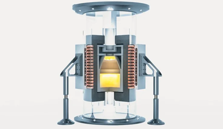
Graphite heaters
semiconductor manufacturing
Mersen’s graphite heaters are known for their high thermal conductivity and resistance to thermal shock. This makes them ideal for applications where uniform heating and temperature stability are essential. Our graphite heaters are used in various semiconductor processes, including epitaxy and silicon crystal growth, where maintaining a controlled temperature is vital for the quality of the final product.
-
Carbon Felt Insulation
high-temperature furnaces
Carbon felt insulation is used in high-temperature furnaces for processes like silicon crystal growth and annealing. Mersen’s carbon felt insulation provides excellent thermal insulation, ensuring energy efficiency and uniform temperature distribution within the furnace.
-
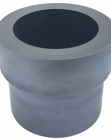
ISO Graphite Crucible
crystal growth processes
Mersen’s isostatic (ISO) graphite crucibles are designed to withstand the extreme temperatures and corrosive environments typical in crystal growth processes. The high purity and structural integrity of ISO graphite crucibles make them ideal for producing high-quality silicon crystals, which are the foundation of semiconductor devices.
-
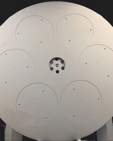
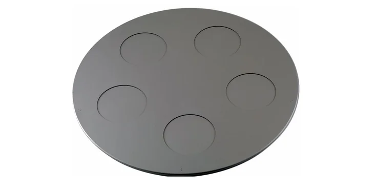
Graphite susceptors
Atomic Layer Deposition (ALD)
Our graphite susceptors provide uniform heat distribution and exceptional thermal stability, which are crucial for the ALD process. These susceptors ensure consistent film quality and thickness, vital for the fabrication of semiconductor devices. Mersen’s graphite susceptors are engineered to withstand the demanding conditions of ALD, offering durability and reliability in a high-precision environment.
-
-
The Importance of PVT in advanced semiconductor manufacturing
PVT is a leading method for fabricating high-quality silicon carbide (SiC) crystals. It involves sublimating silicon and carbon sources to deposit SiC onto a seed crystal in a controlled temperature environment. This process is critical for achieving uniform doping, essential for the wafers' electrical properties. Precise control over the PVT parameters ensures the structural integrity and purity of the crystals, leading to the production of superior wafers.
Depositing elements onto silicon wafers with high precision and uniformity is imperative. This precision is particularly crucial in processes like CVD Silicon Carbide deposition or epitaxial growth, where the electrical characteristics of the semiconductor layers must be tightly controlled. Voltage and temperature parameters must be finely tuned to ensure that the deposited layers have the correct composition and thickness, which are critical for the semiconductor's performance.
Isostatic graphite, carbon/carbon composites and porous graphite are excellent materials for their high-temperature resistance. Managing high temperatures during critical processes such as epitaxy, Chemical Vapor Deposition (CVD), and Physical Vapor Transport (PVT) is essential for the integrity and performance of silicon wafers. High-temperature resilience prevents defects and ensures the structural integrity of wafers, crucial for the efficiency of the final semiconductor device. Mersen's expertise in materials that excel in high-temperature environments positions us as a key supplier for semiconductor manufacturing processes that demand exceptional thermal resistance.
-
SiC semiconductors
Mersen wafer carrier benefits for Silicon and SiC epitaxy
High Purity of Mersen wafer carriers
The high purity of Mersen wafer carriers is essential for preventing contamination during the epitaxial growth process. Any impurities can significantly impact the quality of the semiconductor layers. Mersen's wafer carriers are made from materials, such as graphite, that minimize the risk of contamination, ensuring that the epitaxial layers maintain their desired electrical and physical properties.
Durability of Mersen wafer carriers
The epitaxial process is characterized by exposure to high temperatures, corrosive chemicals, and aggressive cleaning protocols such as in situ cleaning. It can degrade less robust materials. Mersen's carriers are constructed with silicon to withstand these harsh conditions, ensuring a longer lifespan and consistent performance. This durability reduces the need for frequent replacements, thereby lowering operational costs and enhancing the overall efficiency of the semiconductor manufacturing process.
Precision Engineering of Mersen wafer carriers
Precision engineering of wafer carriers is vital for maintaining the uniformity and alignment of wafers during epitaxy. Mersen's wafer carriers are designed with exact specifications to ensure that each wafer is held securely and consistently. This precision is crucial for achieving uniform epitaxial layers and minimizing defects. It is essential for the production of high-quality semiconductor devices. Additionally, the dimensional stability of these carriers under high temperatures and corrosive environments further ensures the integrity of wafer processing. This stability prevents warping or deformation, maintaining precise alignment and uniformity throughout the manufacturing process.
Thermal Stability of Mersen wafer carriers
Thermal stability is a critical feature of Mersen wafer carriers, especially given the high temperatures involved in epitaxial processes. These wafer carriers are engineered to maintain their structural integrity and dimensional stability under thermal stress. This stability is crucial for preventing warping or other deformations that could affect the epitaxial layer quality, ensuring consistent results in semiconductor fabrication.
Corrosion Resistance of Mersen wafer carriers
Corrosion resistance is an essential attribute of Mersen wafer carriers. The epitaxial process can involve exposure to corrosive gases and chemicals. Mersen's wafer carriers are made from isostatic graphite. Isostatic graphite resists corrosion, ensuring that they maintain their integrity and performance over time. This resistance is key to protecting the carriers from degradation, thereby ensuring the purity and quality of the epitaxial layers.
-
SiC semiconductors
Mersen's role in the pioneering SmartSiC™ technology
At Mersen, we are proud to be a key player in the innovative SmartSiC™ technology project. It represents a significant leap forward in the semiconductor industry, particularly in the development and application of silicon carbide (SiC) technologies.
SmartSiC(TM) technology is a groundbreaking approach in the world of silicon carbide substrates. This technology leverages Soitec's SmartCut™ process to create a composite substrate that combines a thin layer of monocrystalline SiC on a polycrystalline SiC substrate provided by Mersen. The result is a substrate with very low electrical resistivity, which is a game-changer in the production of silicon carbide power components, especially for the electric vehicle market.
-
SmartSiC™'s impact on semiconductor efficiency and performance
The unique properties of the SmartSiC™ substrate, including its enhanced thermal conductivity and mechanical strength, lead to significant improvements in the efficiency of silicon carbide power electronics components. This technology allows for the production of semiconductors that are not only more efficient but also more durable, meeting the rigorous demands of high-power applications.
Applications of Soitec's technologies in emerging markets
The electric vehicle industry stands to benefit greatly from these advancements, as SmartSiC™ substrates enable the production of more efficient and compact power electronics. Additionally, these technologies have potential applications in renewable energy systems and industries where many technologies are innovating and emerging.
An approach to sustainable semiconductor manufacturing
Mersen and Soitec's approach to semiconductor manufacturing through SmartSiC(TM) technology is not just about advancing technology; it's also about sustainability. By improving the efficiency and reducing the size of power components, SmartSiC(TM) contributes to the overall reduction of energy consumption and material use in the semiconductor industry. This approach aligns with the global shift towards more sustainable and environmentally friendly manufacturing practices.
How is SmartSiC™ transforming the global semiconductor market?
The SmartSiC™ technology is transforming the global semiconductor market by introducing substrates that are more efficient, cost-effective, and sustainable. This technology is setting new standards in the production of power semiconductors, particularly for the electric vehicle market, and is poised to have a ripple effect across various high-tech industries.
-
Semiconductors
Need to get more info ?
-
Download
Document
Technical documentation
Electronics: Advanced Materials for the Semicon Industry
pdf - 10.27 MB | Nov. 28, 2024


Products
Related Products


News
Related news

Finance
Mersen: European funding for p-SIC®
Learn more
Corporate
Mersen: a major contract with Wolfspeed
Learn more
Corporate